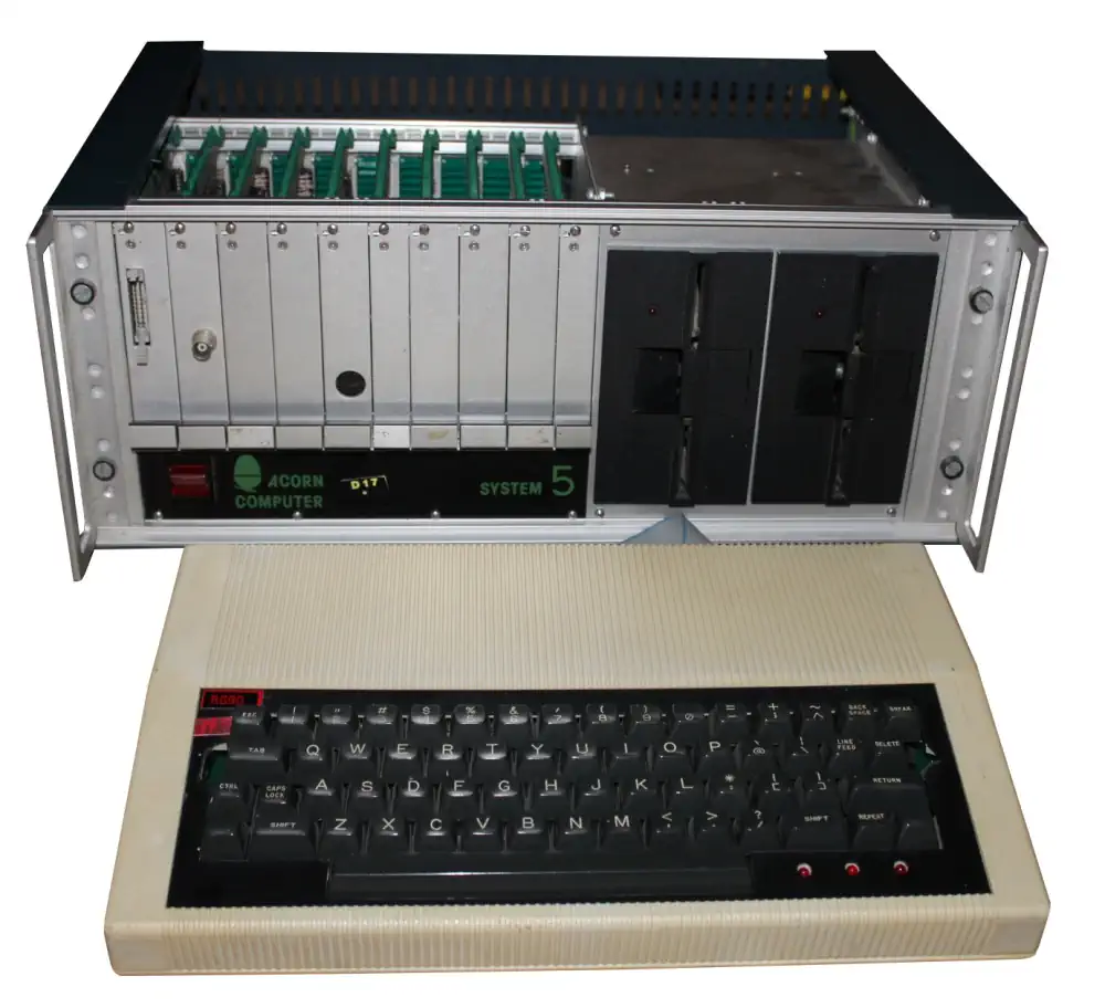

The Acorn System 5
The Acorn System 5, introduced around 1980 by Acorn Computers, was the next step in Acorn’s System-series microcomputers and represented a substantial expansion of the disk-based architecture first seen in the Acorn System 4. Like its predecessor, the System 5 used the MOS Technology 6502 processor and a Eurocard rack format with plug-in boards for memory, I/O, and storage. It typically included floppy disk drives and ran the Acorn Disk Operating System, allowing the machine to load programs and manage files directly from disk rather than cassette.
The main difference between the System 5 and the System 4 was that the System 5 was designed as a multi-user development system rather than a single-user computer. It supported multiple terminals connected to a single central processor through serial interfaces. This allowed several programmers or operators to use the same machine simultaneously, each working from their own terminal while sharing disk storage and system resources. In practical terms, this made the System 5 much better suited for software development environments, schools, and laboratories where several users needed access to the computer at once.
To support this role, the System 5 generally included more RAM capacity, additional I/O cards, and a more sophisticated system configuration than the System 4. Instead of being a workstation attached directly to a monitor and keyboard, it acted more like a small timesharing computer: the rack-mounted computer performed the processing, while users interacted through serial terminals. This shift—from a single-user microcomputer to a small multi-user computing system—was the defining architectural change that distinguished the System 5 from its predecessor.
Acorn System VDU board
The Acorn Visual Display Unit Controller Board connects to the Standard Acorn Computer Bus and contains a memory mapped character storage R.A.M. which is transparently written to or read from by the C.P.U.
An MC6845 programmable controller I.C. provides all the synchronisation signals to drive a 625 line 50 fields per second V.D.U. together with read addresses for the character R.A.M. Characters are then fed to an SAA5050 character generator IC which produces the necessary dot patterns to create the characters to refresh the V.D.U.
The SAA5050 produces Teletext standard characters and has Red, Green and Blue drive outputs giving coloured characters or graphics.
The R.G.B. and sync outputs may be used to drive a colour encoder and modulator for a U.H.F. Television; There is also a 1 volt/75 ohm composite sync and video output which can directly drive a Monochrome Monitor on which the different colours will appear as different scales of grey.
The VDU board came with listings for programs which set up the MC6845, display 25 instructions in hex on the V.D.U. (with double or treble byte instructions on a single line) and allow the drawing of graphics or characters on the V.D.U. These programs may be loaded and run using the Acorn System 1 Monitor. Later new monitor ROM was able to link the VDU and an ASC 11 keyboard to Acorns' 4K Fast BASIC.
The versatility of the programmable MC6845 and the SAA5050 combination may be employed to give other screen formats e. g. 80 characters x 16 lines and double height characters. Thus the Acorn VDU was of great value to experimenters and producers of specialist display systems. The VDU controller PCB was supplied in kit form with a full set of I.C. sockets. It was easily assembled using a small soldering iron and useful hints on assembly may be found in the Acorn Micro-computer System 1 Technical Manual. The board operates from a single +5v supply from which it draws not more than 500 mA.
Motorola MC6845 Video Display Generator
The Motorola MC6845 commonly referred to as a CRTC (Cathode Ray Tube Controller) served as the architectural backbone for the video subsystems of many iconic 8-bit computers, including the IBM PC (CGA/MDA) and the BBC Micro. Unlike modern GPUs that handle complex rendering, the MC6845 was a programmable timing generator. Its primary function was to manage the synchronization signals (HSYNC and VSYNC) and generate the memory addresses required to fetch pixel or character data from video RAM. By offloading these repetitive timing tasks from the CPU, it allowed for flexible display formats through a set of 18 internal 8-bit registers.
At its core, the chip operates using a series of internal counters that track the horizontal and vertical position of the electron beam. The programmer defines the display geometry by writing to registers that control the total number of horizontal characters, the horizontal displayed characters, and the sync pulse widths. This programmability allowed developers to implement various "tricks," such as hardware scrolling or split-screen effects, by manipulating the Start Address Register (R12 and R13) mid-frame. This changed which part of the video memory the controller pointed to at the beginning of a raster scan.
The interface between the MC6845 and the system memory is fundamentally passive regarding data content. The controller outputs a Memory Address (MA0–MA13) and Row Address (RA0–RA4) but it does not actually "see" the data being fetched. In a typical character-mapped configuration, the MA lines point to the character code in RAM, while the RA lines determine which specific scanline of that character is being pulled from a Font ROM. This separation of concerns made it highly versatile, supporting both alphanumeric modes and "all-points-addressable" (APA) graphics modes depending on how the external logic interpreted the address lines.
Timing and synchronization are governed by the Character Clock (CLK) input, which increments the internal horizontal counter. To prevent "snow" or visual artifacts, the system must carefully manage bus contention between the CPU and the MC6845, as both require access to the video RAM. This was often solved using "interleaved" access, where the CPU and CRTC traded cycles, or by restricting CPU writes to the vertical blanking interval. The chip's ability to provide a Light Pen strobe input further expanded its utility, allowing the hardware to latch the current memory address when a light pen hit was detected, providing a primitive but effective form of user interaction.
Programming the MC6845 Video Display Generator
To program the MC6845 for a specific resolution, you must calculate the values for its internal registers based on your system's Character Clock (CLK) and the target monitor's refresh rates. The chip operates by counting character units rather than individual pixels, so your first step is determining how many pixels wide a "character" is (typically 8) to find your horizontal frequency.
1. Horizontal Timing Registers (R0–R3)
These registers define the width of the scanline and the position of the horizontal sync pulse (HSYNC).- R0 (Horizontal Total): The total number of character clocks in a full scanline, including the visible area and the "overscan/blanking" period.
- R1 (Horizontal Displayed): The number of characters actually shown on the screen (e.g., 40 or 80).
- R2 (Horizontal Sync Position): This determines where the sync pulse starts. Moving this value shifts the entire image left or right on the monitor.
- R3 (Sync Width): Defines the duration of the HSYNC pulse in character clock units.
2. Vertical Timing Registers (R4–R7)
Vertical timing is measured in character rows not individual scanlines.- R4 (Vertical Total): The total number of character rows in a frame.
- R5 (Vertical Total Adjust): A "fine-tuning" register that adds a specific number of scanlines to the end of a frame to reach exactly 50Hz or 60Hz if the character rows don't divide perfectly.
- R6 (Vertical Displayed): The number of visible rows on the screen (e.g., 25).
- R7 (Vertical Sync Position): Determines the vertical start of the sync pulse, effectively moving the image up or down.
3. Character and Scanline Control (R9–R11)
The MC6845 needs to know the physical "height" of your characters to correctly increment its addresses.- R9 (Maximum Scan Line Address): This tells the chip how many scanlines make up one character row (e.g., 7 for an 8-pixel high character, as the count starts at 0).
- R10 & R11 (Cursor Control): These define which scanlines within a character block the cursor occupies and whether it should blink.
4. Memory Mapping (R12–R13)
These are the Start Address Registers They determine which byte in your Video RAM corresponds to the very first character at the top-left of the screen. By changing these values during a "Vertical Blank" period, you can achieve Hardware Scrolling If you increment the start address by the width of one row, the screen appears to jump up instantly without the CPU having to move a single byte of data in memory.CPU - The Motorola 6502
The 6502 is an 8-bit MicroProcessor designed by MOS Technology. The team was led by Chuck Peddle and had also worked on the Motorola 6800. The 6502 is a simplified, but faster and cheaper design than the 6800.
The 6502 was introduced in 1975 and was the cheapest microprocessor on the market. Together with the Zilog Z80, the 6502 helped start the home computer revolution of the 1980s. The 6502 was used in a wide range of devices: the Atari 2600, the 8-bit Atari home computers, the Apple II, the Nintendo Entertainment System, the Commodore 64, the BBC Micro and many others. All used the 6502 or a variation of it.
The 6502 is a 1MHz design, while the 6502A is designed for 2MHz. The 6502A is 100% compatible with the original 6502.
Commodore soon bought MOS Technology, but conitnued to sell the microprocessor to competitors and licensed the design to other manufacturers.
Source: WikiPedia - MOS Technology 6502The 650x Instruction Set
| Mnemonic | Operation | Description |
|---|---|---|
| ADC | Add with Carry | Adds a memory location and the carry bit to the accumulator. |
| AND | Logical AND | Performs a logical AND between memory and the accumulator. |
| ASL | Arithmetic Shift Left | Shifts all bits one position to the left (in memory or accumulator). |
| BCC | Branch on Carry Clear | Branches to a new address if the carry flag is clear (0). |
| BCS | Branch on Carry Set | Branches to a new address if the carry flag is set (1). |
| BEQ | Branch on Equal (Zero Set) | Branches to a new address if the zero flag is set (1). |
| BIT | Bit Test | Tests bits in memory with the accumulator without modifying the accumulator. |
| BMI | Branch on Minus | Branches to a new address if the negative flag is set (1). |
| BNE | Branch on Not Equal | Branches to a new address if the zero flag is clear (0). |
| BPL | Branch on Plus | Branches to a new address if the negative flag is clear (0). |
| BRK | Force Break | Forces an interrupt request and pushes status and PC to the stack. |
| BVC | Branch on Overflow Clear | Branches to a new address if the overflow flag is clear (0). |
| BVS | Branch on Overflow Set | Branches to a new address if the overflow flag is set (1). |
| CLC | Clear Carry Flag | Clears the processor carry flag. |
| CLD | Clear Decimal Mode | Clears the processor decimal mode flag. |
| CLI | Clear Interrupt Disable | Clears the interrupt disable flag, allowing maskable interrupts. |
| CLV | Clear Overflow Flag | Clears the processor overflow flag. |
| CMP | Compare Accumulator | Compares the contents of a memory location with the accumulator. |
| CPX | Compare X Register | Compares the contents of a memory location with the X register. |
| CPY | Compare Y Register | Compares the contents of a memory location with the Y register. |
| DEC | Decrement Memory | Subtracts one from the value held at a specified memory location. |
| DEX | Decrement X Register | Subtracts one from the X register. |
| DEY | Decrement Y Register | Subtracts one from the Y register. |
| EOR | Exclusive OR | Performs a logical Exclusive OR between memory and the accumulator. |
| INC | Increment Memory | Adds one to the value held at a specified memory location. |
| INX | Increment X Register | Adds one to the X register. |
| INY | Increment Y Register | Adds one to the Y register. |
| JMP | Jump | Sets the program counter to a new address. |
| JSR | Jump to Subroutine | Pushes the return address to the stack and jumps to a new address. |
| LDA | Load Accumulator | Loads a byte of memory into the accumulator. |
| LDX | Load X Register | Loads a byte of memory into the X register. |
| LDY | Load Y Register | Loads a byte of memory into the Y register. |
| LSR | Logical Shift Right | Shifts all bits one position to the right (in memory or accumulator). |
| NOP | No Operation | Performs no operation, consuming 2 machine cycles. |
| ORA | Logical Inclusive OR | Performs a logical OR between memory and the accumulator. |
| PHA | Push Accumulator | Pushes a copy of the accumulator onto the stack. |
| PHP | Push Processor Status | Pushes a copy of the status flags onto the stack. |
| PLA | Pull Accumulator | Pulls a byte from the stack into the accumulator. |
| PLP | Pull Processor Status | Pulls a byte from the stack into the processor status flags. |
| ROL | Rotate Left | Rotates all bits one position left through the carry flag. |
| ROR | Rotate Right | Rotates all bits one position right through the carry flag. |
| RTI | Return from Interrupt | Pulls the processor flags and program counter from the stack. |
| RTS | Return from Subroutine | Pulls the program counter from the stack and resumes execution. |
| SBC | Subtract with Carry | Subtracts memory and the inverse of the carry bit from the accumulator. |
| SEC | Set Carry Flag | Sets the processor carry flag. |
| SED | Set Decimal Flag | Sets the processor decimal mode flag. |
| SEI | Set Interrupt Disable | Sets the interrupt disable flag, preventing maskable interrupts. |
| STA | Store Accumulator | Stores the contents of the accumulator in memory. |
| STX | Store X Register | Stores the contents of the X register in memory. |
| STY | Store Y Register | Stores the contents of the Y register in memory. |
| TAX | Transfer Accumulator to X | Copies the current value of the accumulator into the X register. |
| TAY | Transfer Accumulator to Y | Copies the current value of the accumulator into the Y register. |
| TSX | Transfer Stack Pointer to X | Copies the current value of the stack pointer into the X register. |
| TXA | Transfer X to Accumulator | Copies the current value of the X register into the accumulator. |
| TXS | Transfer X to Stack Pointer | Copies the current value of the X register into the stack pointer. |
| TYA | Transfer Y to Accumulator | Copies the current value of the Y register into the accumulator. |
ROM: 6kB