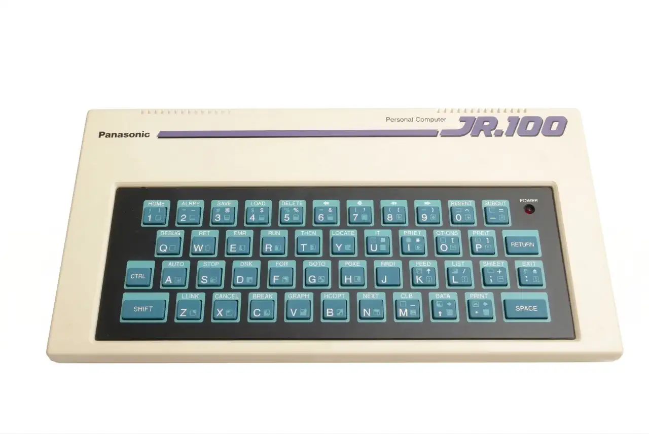

The Panasonic JR-100, released in 1981, was an entry-level 8-bit home computer designed to be an affordable introduction to programming. At its core, it utilized the Motorola MC6802 microprocessor, a variant of the popular 6800, running at a clock speed of approximately 0.89 MHz The system was equipped with 16 KB of RAM which was relatively generous for a budget machine of its era, though it was expandable up to 32 KB via an external memory unit. Its firmware was housed in an 8 KB ROM, which contained a custom version of JR-BASIC, allowing users to begin coding immediately upon powering up.
In terms of visual output, the JR-100 featured a specialized video controller capable of displaying 32 columns by 24 lines of text. It did not support high-resolution bitmapped graphics in the modern sense; instead, it relied on a set of 64 built-in alphanumeric characters and 64 user-definable semi-graphic symbols. This allowed for a pseudo-resolution of 64 x 48 blocks The display was strictly monochrome (black and white), which helped keep the hardware costs low but limited its appeal compared to color-capable rivals like the VIC-20 or the ZX Spectrum.
The audio capabilities of the JR-100 were basic, featuring a single-channel internal speaker driven by a simple frequency generator. It was capable of producing square-wave beeps across a range of several octaves, primarily used for simple melodies or user feedback in BASIC programs. For data storage, the unit featured a standard 1200-baud cassette interface allowing programs to be saved to and loaded from any standard tape recorder. Despite its technical constraints, the JR-100’s unique "chiclet" style rubber keyboard and compact, all-in-one design made it a notable, if short-lived, piece of early computing history.
Video Generation Circuitry
The Panasonic JR-100 did not use a standard off-the-shelf "Video Display Controller" (VDC) like the common Motorola 6845 or TMS9918 found in many of its contemporaries. Instead, its video generation was handled by a combination of discrete logic and a custom gate array or specialized interface chip.
While the JR-100’s specific video logic is often just referred to as a "custom video controller" in many technical summaries, deeper hardware documentation identifies a key component:
- The Chip: The HD61K201F (on NTSC models) or HD61L204F (on other variants).
- Function: This was a specialized CMOS gate array manufactured by Hitachi. It served as the system's "traffic controller," managing the timing for the CPU, generating the clock signals, and handling the address decoding required to output the text and semi-graphic data to the screen.
How it worked
Unlike a true graphics chip that might have its own dedicated hardware sprites or high-resolution modes, this controller was essentially a high-speed character generator. It pulled data from the 2 KB of Video RAM (VRAM)—typically comprised of two HM6116 static RAM chips—and translated that into the 32x24 monochrome grid you saw on your monitor.Because it lacked a dedicated bitmapped graphics processor, any "drawing" had to be done by manipulating the 64 user-definable characters, which the controller would then render as a grid of pixels.
Simulation of higher resolution graphics
The way the JR-100 handled "high-resolution" graphics was a clever bit of engineering designed to bypass its lack of a true bitmapped mode. Instead of the CPU controlling every single pixel on the screen (which would have required more memory and a more expensive video chip), the HD61K201F controller used User-Definable Characters (UDC).
Here is how that process worked:
1. The Grid System
The screen was divided into a fixed grid of 32 x 24 character cells. Normally, each cell would display a letter like "A" or a number like "5" pulled from the internal ROM. However, the system allowed you to tell the video controller to look at a specific area of RAM instead of the ROM for certain character codes.2. Custom Pixel Patterns
Each character cell was an 8 x 8 pixel block. By using the POKE command in BASIC, a programmer could rewrite the 8 bytes of data associated with a UDC.
- Each byte represented one horizontal row of 8 pixels.
- A "1" in a bit position turned a pixel on, and a "0" turned it off.
3. Simulating "Bitmapped" Graphics
By defining a set of these custom characters as different patterns of dots, lines, or shapes, you could "paint" a complex image across the 32x24 grid.
For example, if you wanted to draw a diagonal line, you wouldn't tell the computer "draw a line from X to Y." Instead, you would:
- Define a character that looked like a small diagonal segment.
- Place that character in the specific grid coordinates (e.g., Column 5, Row 10) where the line needed to pass through.
4. Memory Efficiency
The brilliance of this approach was memory conservation. A full 256 x 192 bitmap (common on other systems) would require 6,144 bytes of VRAM. By using the UDC method, the JR-100 only needed 2,048 bytes to manage the entire screen. This left more of the 16 KB RAM available for the user's actual program code.
The 8-bit CMOS MN1800A processor
The MN1800A is an 8-bit CMOS microprocessor manufactured by Panasonic (then Matsushita) in the early 1980s.
It is most famous for being a "clone" or highly compatible variant of the Motorola 6802 (which was itself an improved version of the legendary Motorola 6800). If you are familiar with the 6800 family of processors—which powered early industrial equipment and computers like the Altair 680—you’ll find the MN1800A very similar in architecture.
Key Technical Specifications
The MN1800A was designed for home computers and embedded control systems. Here is a breakdown of its core characteristics:
- Word Size: 8-bit data bus.
- Address Space: 16-bit address bus (capable of addressing up to 64 KB of memory).
- Clock Speed:Typically ran around 0.89 MHz to 1 MHz (though the "A" variant could technically handle up to 1.5 MHz).
- Instruction Set: Compatible with the Motorola 6802. It includes 72 instructions with various addressing modes.
- Internal Registers:
- Two 8-bit Accumulators (A and B): Used for arithmetic and logic operations.
- 16-bit Index Register (X): Used for memory addressing.
- 16-bit Stack Pointer (S) and Program Counter (PC).
The most prominent use of the MN1800A was as the main CPU for the Panasonic (National) JR-200 home computer released in 1982.
Interestingly, in that system, the MN1800A didn't work alone. It was paired with a secondary 4-bit processor (the MN1544CJR) that handled input/output (I/O) tasks like managing the keyboard and generating sound. This "dual-processor" setup allowed the MN1800A to focus more on running programs and processing logic.
Comparison: MN1800A vs. Motorola 6802
While they are functionally almost identical, there is one major hardware difference:- Motorola 6802: Has an internal clock oscillator.
- Panasonic MN1800A: Does not have an internal oscillator; it requires an external clock signal to be provided to the chip.
RAM max: 32kByte
ROM: 8kB
VRAM: 2kB
2kB for graphic characters
2kB VRAM
64x48 semi graphics (256x192 virtual graphics)
16x16
8/scanline
64 total